|
R&D Center
 |
R&D Center
Current Position:HOME > R&D Center > Testing Platform
S4800 Field emission SEM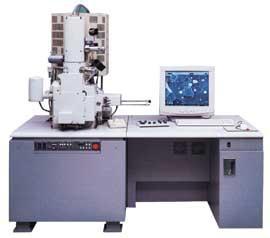
This machine is widely used in all kinds of metal materials and non-metallic materials testing
and research. In many fields of scientific research materials , metal materials, chemical materials, semiconductor materials , ceramic materials , etc., it may conduct material microstructure observation, organization, component analysis, material fracture analysis and failure analysis ; morphology observed organize various materials ; materials real-time micro- component analysis ; rapid multi-element surface scan and line scan distribution measurements ; grain size , shape analysis , crystal , crystal orientation measurement ; elements of qualitative and quantitative composition analysis ; phase identification crystal grains. Technical parameters: Secondary electron Resolution : 1.4nm (1 kV, deceleration mode ) 1.0nm (15kV) Electron optics : Electron gun: cold field emission electron source Acceleration voltage : 0.5 ~ 30kV (0.1KV / step variable ) Magnification : x 20 ~ x 800,000 Lens aperture : 4 holes , vacuum outside the selection and adjustment ( built-in heater ) Detector: secondary electron detector ( high / low ) transmission electron detector cathode fluorescent detector Faraday cup The sample stage : l Type : X: 0 ~ 50mm Y: 0 ~ 50mm Z: 1.5 ~ 30mm T: -5 ~ +70 ° R: 360 ° Driver : manual ( optional 3 -axis drive ) Scan Mode : Standard , Split / dual mag / line scan, position set, spot, AAF, SAA, oblique. Screen Storage : 640 x 480, 1,280 x 960, 2,560 x 1,920,5,120 x 3,840 Scan speed : TV, slow (0.5 ~ 40 s / frame ) used to observe a slow (40 ~ 320 s / frame ) for recording Imaging process : automatic adjustment of brightness and contrast Raster rotation, auto focus, auto astigmatism correction , Average , frame integration , pseudo-color display Automatic data record: No film , accelerating voltage , micron scale magnification , date , time, working distance Electronic image movement : ± 12u (W.D. = 8 mm)
Main features:
1-A new objective lens design with "Super ExB Filter" technology. Using a single detector, the Super ExB Filter collects and separates the various components of pure SE, compositional SE and BSE electron signals. 2-A guaranteed resolution of 1.4 / 2.0 nm at 1kV (deceleration / standard mode) for low voltage applications. 3-Type II specimen stage for large sample applications with 110mm x 110mm stage movement and computer controlled 5 axes motorization with graphical interface software.
|
| Copyright © Suzhou Saifei Group Ltd. All rights reserved. ICP: 13061365-1 |
|
|